decimal code를 7 segment 신호로 변환하는 회로는 사실 case문 써서 그냥 0~9일때 {A, B, C, D, E, F, G}의 값을 전부 지정할 수도 있지만, 이번에는 4 to 16 decoder를 써볼까 한다.
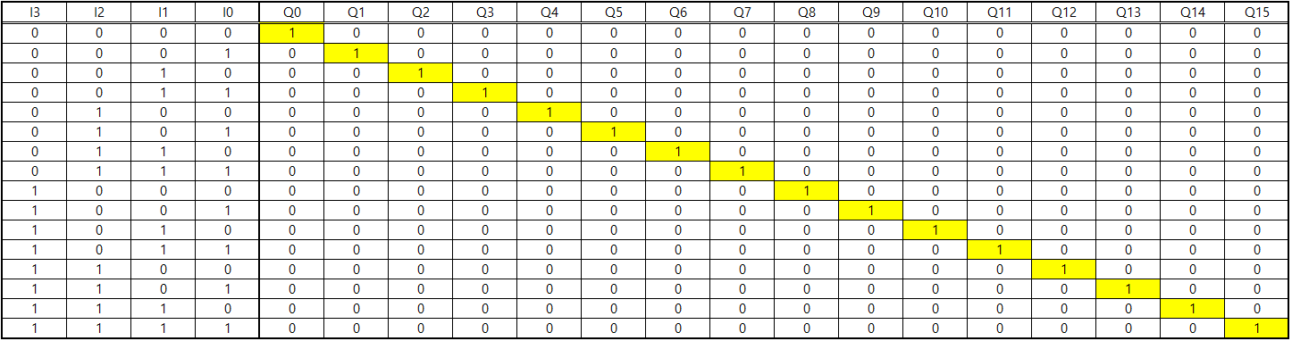
4 to 16 decoder는 4비트 인풋이 들어오면 16개의 아웃풋 포트 중 한 포트만 1, 나머지는 0이 되는 속성을 지니고 있다.
이말은 즉 16개의 신호를 적당히 OR 연산을 취하면 7 segment 신호를 만들 수 있다는 것이다.

왼쪽 사진과 같은 7 segment에서(DP는 무시한다.) {I3, I2, I1, I0}가 b'0001일 경우 B와 C만 1이고 나머지는 0이다. 이를 임시로 아래와 같이 나타낼 수 있다.
B = Q1 | ???
C = Q1 | ???
b'0000일 때는 G를 제외한 나머지가 전부 1이다. 앞에 식에서 덧붙이면 아래와 같다.
A = Q0 | ???
B = Q0 | Q1 | ???
C = Q0 | Q1 | ???
D = Q0 | ???
E = Q0 | ???
F = Q0 | ???
G = ???
그럼 b'0010 일때는? A, B, G, E, D에 Q2를 추가로 OR 연산을 취하면 될 것이다. 그럼 b'0011일떄는? A, B, C, D, G 에 추가해야 될 것이다. 이렇게 할 수 있는 이유는 Q0~15가 하나씩만 1이기 때문이다.
이제 어떻게 설계할지 알 수 있을 것이다. 아래와 같이 설계하면 된다.
module bcd_to_7seg(
    input [3:0] bcd_in,
    output [6:0] seg7_out
);

wire [15:0] decoder_out;
wire Error = |decoder_out[15 -: 6];

dec_4to16 DECODER(bcd_in, decoder_out);

assign seg7_out[0] = decoder_out[0] |
                     decoder_out[2] |
                     decoder_out[3] |
                     decoder_out[5] |
                     decoder_out[6] |
                     decoder_out[7] |
                     decoder_out[8] |
                     decoder_out[9] |
                     Error;             // A

assign seg7_out[1] = decoder_out[0] |
                     decoder_out[1] |
                     decoder_out[2] |
                     decoder_out[3] |
                     decoder_out[4] |
                     decoder_out[6] |
                     decoder_out[7] |
                     decoder_out[8] |
                     decoder_out[9];    // B

assign seg7_out[2] = decoder_out[0] |
                     decoder_out[1] |
                     decoder_out[3] |
                     decoder_out[4] |
                     decoder_out[5] |
                     decoder_out[6] |
                     decoder_out[7] |
                     decoder_out[8] |
                     decoder_out[9];    // C

assign seg7_out[3] = decoder_out[0] |
                     decoder_out[2] |
                     decoder_out[3] |
                     decoder_out[5] |
                     decoder_out[6] |
                     decoder_out[8] |
                     decoder_out[9] |
                     Error;             // D

assign seg7_out[4] = decoder_out[0] |
                     decoder_out[2] |
                     decoder_out[6] |
                     decoder_out[8] |
                     Error;             // E

assign seg7_out[5] = decoder_out[0] |
                     decoder_out[4] |
                     decoder_out[5] |
                     decoder_out[6] |
                     decoder_out[8] |
                     decoder_out[9] |
                     Error;             // F

assign seg7_out[6] = decoder_out[2] |
                     decoder_out[3] |
                     decoder_out[4] |
                     decoder_out[5] |
                     decoder_out[6] |
                     decoder_out[8] |
                     decoder_out[9] |
                     Error;             // G

endmodule
module dec_4to16(
    input [3:0] data_in,
    output [15:0] Q_out
);

wire [3:0] I, J;

assign I[0] = data_in[0];
assign I[1] = data_in[1];
assign I[2] = data_in[2];
assign I[3] = data_in[3];

assign J[0] = ~I[0];
assign J[1] = ~I[1];
assign J[2] = ~I[2];
assign J[3] = ~I[3];

assign Q_out[0]  = J[3] & J[2] & J[1] & J[0]; // 0 0 0 0
assign Q_out[1]  = J[3] & J[2] & J[1] & I[0]; // 0 0 0 1
assign Q_out[2]  = J[3] & J[2] & I[1] & J[0]; // 0 0 1 0
assign Q_out[3]  = J[3] & J[2] & I[1] & I[0]; // 0 0 1 1
assign Q_out[4]  = J[3] & I[2] & J[1] & J[0]; // 0 1 0 0
assign Q_out[5]  = J[3] & I[2] & J[1] & I[0]; // 0 1 0 1
assign Q_out[6]  = J[3] & I[2] & I[1] & J[0]; // 0 1 1 0
assign Q_out[7]  = J[3] & I[2] & I[1] & I[0]; // 0 1 1 1
assign Q_out[8]  = I[3] & J[2] & J[1] & J[0]; // 1 0 0 0
assign Q_out[9]  = I[3] & J[2] & J[1] & I[0]; // 1 0 0 1
assign Q_out[10] = I[3] & J[2] & I[1] & J[0]; // 1 0 1 0
assign Q_out[11] = I[3] & J[2] & I[1] & I[0]; // 1 0 1 1
assign Q_out[12] = I[3] & I[2] & J[1] & J[0]; // 1 1 0 0
assign Q_out[13] = I[3] & I[2] & J[1] & I[0]; // 1 1 0 1
assign Q_out[14] = I[3] & I[2] & I[1] & J[0]; // 1 1 1 0
assign Q_out[15] = I[3] & I[2] & I[1] & I[0]; // 1 1 1 1

endmodule
module tb_7seg();

reg [3:0] bcd_input;
wire [6:0] seg7_output;

bcd_to_7seg TEST(bcd_input, seg7_output);

initial begin
    bcd_input <= 4'd0;
    #10
    bcd_input <= 4'd1;
    #10
    bcd_input <= 4'd2;
    #10
    bcd_input <= 4'd3;
    #10
    bcd_input <= 4'd4;
    #10
    bcd_input <= 4'd5;
    #10
    bcd_input <= 4'd6;
    #10
    bcd_input <= 4'd7;
    #10
    bcd_input <= 4'd8;
    #10
    bcd_input <= 4'd9;
    #10
    bcd_input <= 4'd10; // Error start
    #10
    bcd_input <= 4'd11;
    #10
    bcd_input <= 4'd12;
    #10
    bcd_input <= 4'd13;
    #10
    bcd_input <= 4'd14;
    #10
    bcd_input <= 4'd15;
    #10
    $finish;
end

endmodule
아까 설명했던대로 1인 경우에만 OR을 취하면 되는 간단한 회로다.
시뮬레이션을 돌려보면 아래와 같이 나오는데, 실제 7segment 출력 파형과 똑같다.

이미지 출처
https://en.wikipedia.org/wiki/Seven-segment_display
'Verilog HDL 설계' 카테고리의 다른 글
| 테스트벤치 작성 예시 (0) | 2021.04.25 |
|---|---|
| Countdown control & display (0) | 2021.04.23 |
| 간단한 Deinterleaver (0) | 2021.04.18 |
| D latch, Master-Slave D flip-flop 구현 (gate level) (0) | 2021.04.17 |
| 8bit Binary to BCD (0) | 2021.04.14 |


